Why use an operational amplifier? This post will demonstrate voltage follower, comparator, and amplifier circuits and provide the governing equations. For ease of understanding the circuits, we will pretend that the op amp is ideal. The non-ideal effects will be added via superposition in a future post.
Click here for the full Guide to Practical Operational Amplifiers.
Voltage Follower (or Buffer) Circuit
The voltage follower circuit is used to buffer a signal for the next stage or to drive an output. A pure voltage follower is not commonly implemented because other components can be added for additional functionality (such as gain, filtering, etc.). Note that the voltage follower uses negative feedback and has unity gain.
With the voltage follower, the output equals the input.


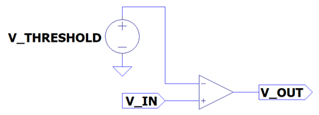
Comparator Circuit
The output of the comparator is a Boolean value based on the input compared to a threshold voltage. Depending on the input value, the output will be one of the two supply rails. Practical implementation of the comparator circuit is usually not this simple. To help prevent noise on the input from causing the output to “bounce”, a feedback network with hysteresis is typically implemented. This will be discussed in a future post.
Note that while this is a non-inverting configuration, an inverting configuration could also be designed.


where, VCC equals the op amp’s positive supply voltage and VEE equals the op amp’s negative supply voltage.
Amplifier Circuits
The inverting and non-inverting amplifiers are the building blocks of most op amp circuits. You should memorize their transfer functions. The arithmetic op amp circuits in the next post will be characterized by using these transfer functions and applying the concept of superposition.
Inverting Amplifier
The inverting amplifier will buffer a signal with gain or attenuation, and the output of the circuit will have a 180° phase shift. In simpler terms, gain (greater than one, unity, or less than one) can be applied, and the output will be inverted.
The advantage of the inverting configuration is that the common mode voltage is constant, and the input is protected by the resistance of the input resistor. Gain will simply be the negate of the ratio of the resistor in the feedback path (RF) over the input resistor (RI) and can be from zero to infinity.


Gain Demo
This demonstration sets up an inverting op amp circuit where VIN is a 1kHz sinusoidal input of 2mVPP. The feedback resistor (RF) is set to 750kΩ, and the input resistor (RI) is set to 6.98kΩ.
Based on the inverting amplifier equation above, the gain of this circuit can be calculated as:

To run the demonstration…
- Make sure you have LTSpice® installed. You can download the latest version at https://www.analog.com/en/design-center/design-tools-and-calculators/ltspice-simulator.html.
- Download and open Gain Demo.asc in LTSpice®.
- Run the simulation.
- Press “Ctrl+L” to view the output.
In a new window, you should see text similar to the following:
vout_pp: PP(v(vout))=0.214267 FROM 0 TO 0.01
gain: vout_pp/vin_pp=107.134
LTSpice® calculates the gain as the peak-to-peak output voltage divided by the peak-to-peak input voltage. The simulated gain very closely matches our result from equation . However, LTSpice® calculates a positive number because the peak-to-peak calculation produces an absolute value.
- Start increasing the input voltage.
At what point does the output start to clip? What happens to the gain when the output is clipped? This demonstrates the non-ideal, finite gain of the op amp as limited by the supply voltage.
Non-Inverting Amplifier
The non-inverting amplifier will buffer a signal with gain. With the non-inverting topology, attenuation is not possible – gain is always at least one. The advantage of the non-inverting amplifier is that the signal is not inverted and the input is directly into the op amp. The latter is beneficial since the input impedance into the op amp is high.


Comments are closed