This post covers the other most commonly used op amp circuits. Basic math functions such as addition and subtraction can accomplished with op amps. Basic analog filters and an integrator demo are also discussed.
Click here for the full Guide to Practical Operational Amplifiers.
Arithmetic Functions
Summing Circuit
The summing circuit allows you to add two or more voltages together. To solve for the output, consider each inverting input on its own using the concept of superposition. The result is in an output term for each input where the input has the same inverting gain term as in the equation for an inverting amplifier (refer to part 1 of this post).
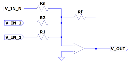

The above figure shows this circuit with the non-inverting input node (V+) of the op amp connected to ground. How would the output of this circuit be affected if a voltage was applied to the non-inverting input? Using superposition, you would add that voltage as a non-inverting gain term (refer to part 1 of this post) where the input resistance (RI) is all of the input resistances (R1, R2, … Rn) in parallel.


Differencing Circuit
The differencing circuit allows you to subtract one voltage from another. It is particularly useful when your application calls for converting a differential analog signal to a single ended signal. Superposition is once again used to solve for the output. The gain term for the VIN- input is the inverting term from equation for an inverting amplifier. To calculate the output term for the VIN+ input, consider R3 and R4 as a voltage divider. Then, the gain term from the equation for a non-inverting amplifier can be used for the non-inverting input (V+).
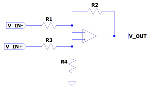

This circuit and the resulting equation can be simplified by making the following restrictions on resistor values.


Then, the output of the circuit becomes the difference of the inputs multiplied by a gain that is the ratio of R2 to R1. Here, gain or attenuation of the difference can be achieved.

Analog Filters
The analog filters section is included to provide baseline knowledge for the non-ideal op amp operation discussions later on. Only basic equations for the first order op amp filters are shown as the full details of analog filter design and characterization are out of scope for this guide. More information on analog filter design can be found readily available both online and in print. Maxim Integrated™ tutorials 733 and 1795 are good starting points.
High Pass Filter (Differentiator)
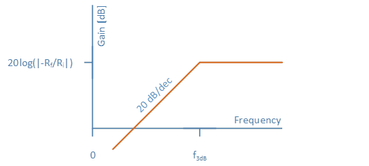
The High Pass Filter (HPF) blocks DC signals and amplifies AC signals. It also functions as a differentiator where the output approximates the derivative of the input. The first order, high pass, op amp filter is shown here along with its frequency response.



Low Pass Filter (Integrator)
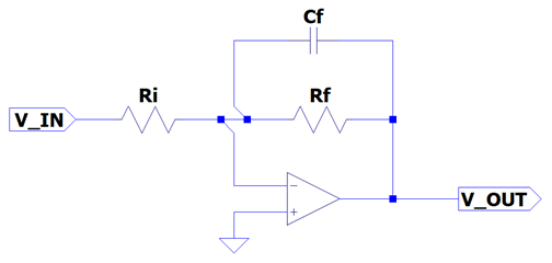
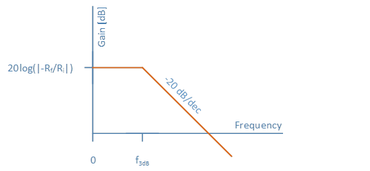
The Low Pass Filter (LPF) limits the bandwidth of the signal by allowing DC and near-DC signals to pass while attenuating high frequency signals. It also can be used to perform the integral of the input signal. This makes it a useful mathematical function that can convert a square wave to a triangle wave, acceleration to velocity, velocity to position, etc. Low Pass Filters are also used to perform anti-aliasing functions. The first order, low pass, op amp filter is shown here along with its frequency response.


LPF and Integrator Demo
This demonstration sets up a first order, active, low pass filter where VIN is a 100Hz sinusoidal input of 500mVPP. The feedback resistor (RF) is set to 69.8kΩ, and the input resistor (RI) is set to 6.98kΩ. The capacitor has a value of 1000pF.
Based on the above LPF equations, the transfer function is:

At 100Hz the gain is:

Using the above LPF equations, the 3dB corner frequency is:

To run the demonstration…
- Download and open LPF Demo.asc in LTSpice® and run the simulation.
- Press “Ctrl+L” to view the output. It should be similar to the following:
vout_pp: PP(v(vout))=4.98976 FROM 0 TO 0.1
gain: vout_pp/vin_pp=9.97952
The simulated gain very closely matches our calculated gain.
- Change the input frequency to that of the 3dB corner frequency and re-run the simulation.
- Press “Ctrl+L” to view the new output. It should be similar to the following:
vout_pp: PP(v(vout))=3.60998 FROM 0 TO 0.1
gain: vout_pp/vin_pp=7.21996
The gain at the 3dB corner frequency can be calculated as 7.07. The simulated gain at this corner frequency closely matches the expected value.
- Use LTSpice® to plot the waveforms of both VOUT and VIN. You should notice a 90° phase shift between the two. This is introduced by the integration function of this circuit.
- Reconfigure the VIN source in the demo circuit to generate a square wave at the 3dB corner frequency. This can be done by right clicking on the VIN source, selecting PULSE, and entering the following options:
| Vinitial [V] | Von [V] | Tdelay [s] | Trise [s] | Tfall [s] | Ton [s] | Tperiod [s] |
|---|---|---|---|---|---|---|
| -0.25 | 0.25 | 0 | 0.01u | 0.01u | 219u | 439u |
- Re-run the simulation and plot the waveforms of both VOUT and VIN. Compare the difference in shape between the output and input signals. Why did the shape change? This shows that the integration of a square wave produces a triangle wave.
Comments are closed